What Are The Characteristics Of A Photovoltaic Cell?
A photovoltaic cell, often referred to as a solar cell, is a device that converts light energy into electricity using the photovoltaic effect. The photovoltaic effect refers to the generation of voltage and electric current in a material upon exposure to light. It was first observed in 1839 by French physicist Edmond Becquerel.
Photovoltaic cells have become an important technology for generating renewable electricity from sunlight. When sunlight (photons) strikes a photovoltaic cell, it excites electrons and causes them to flow, generating an electric current that can be captured and used as electricity. Photovoltaic panels, which contain many linked photovoltaic cells, are assembled into solar arrays that can range from small rooftop systems to large utility-scale solar farms.
Photovoltaic electricity generation is now a rapidly growing industry worldwide. It offers a green solution for obtaining energy from sunlight rather than fossil fuels. Photovoltaic solar energy holds great promise for meeting the world’s rising energy needs in a sustainable manner.
Semiconductor Materials
The most common semiconductor material used in photovoltaic cells is silicon. Silicon is abundant, inexpensive, and can be processed into a crystalline structure optimized for absorbing photons. However, silicon has an indirect bandgap which means it is not as efficient at converting sunlight into electricity compared to materials with a direct bandgap.
Other semiconductor materials like gallium arsenide, cadmium telluride, and copper indium gallium selenide have higher efficiency potential thanks to their direct bandgaps. Gallium arsenide tends to be used for specialty applications where cost is less of a concern, such as space satellites. Cadmium telluride offers good efficiency with lower costs compared to silicon, but the toxicity of cadmium can create environmental concerns. Copper indium gallium selenide (CIGS) has emerged as a leading thin-film solar cell material, combining high efficiency with low materials costs.
PN Junction
A PN junction forms the core of a photovoltaic cell. It consists of two semiconductor regions – one positively doped (p-type) and one negatively doped (n-type). When these two regions are brought into contact, a diffusion of charge carriers takes place.
The negatively charged electrons from the n-type region diffuse into the p-type region. Similarly, the positively charged holes from the p-type region diffuse into the n-type region. This diffusion of charge carriers leads to a charge imbalance across the junction, creating an electric field directed from the positive (p-type) side to the negative (n-type) side.
This electric field creates a drift current opposite to the diffusion current. At equilibrium, the drift and diffusion currents balance out such that the net current across the junction is zero. The regions near the junction become depleted of their majority charge carriers, creating the depletion region. The built-in potential of the PN junction causes photo-generated electrons and holes to drift in opposite directions.
Absorption of Light
When sunlight hits a solar cell, the photons in the sunlight are absorbed by the semiconductor material. This photon absorption causes electrons in the material’s atoms to become excited and jump from a lower energy level to a higher one. The excited electrons leave behind holes where they were originally located.
The amount of sunlight absorbed depends on the material’s bandgap energy. The bandgap energy is the minimum energy required to excite an electron from the valence band to the conduction band. Photons with energy less than the bandgap pass through the material without being absorbed. Those with energy greater than the bandgap are absorbed, but their excess energy is lost as heat.
Silicon is commonly used in solar cells and has a bandgap energy of 1.1 eV. This means it absorbs photons with wavelengths up to about 1100 nm, covering most of the solar spectrum. Other semiconductor materials like GaAs have higher bandgaps and can absorb photons with shorter wavelengths.
By tuning the bandgap energy through material engineering, solar cell designers can optimize sunlight absorption for improved efficiency.
Electric Field
When light hits the photovoltaic cell, it excites electrons in the semiconductor material, causing them to break free from their atoms. This generates electron-hole pairs in both the n-type and p-type regions of the PN junction.
The key to generating electricity is the internal electric field created across the PN junction. When the two differently doped semiconductor materials are brought together, electrons diffuse from the n-type side to the p-type side. This leaves behind positive ion cores on the n-side, and negative electrons accumulating on the p-side.
This diffusion of electrons creates a charge imbalance and thus an electric field pointing from the positive p-side to the negative n-side. This internal electric field provides the driving force to separate the photogenerated electron-hole pairs before they can recombine.
The electric field causes electrons to drift to the n-side and holes to drift to the p-side. This separation of charge carriers across the PN junction is critical to generating a voltage and electric current.
Charge Carrier Collection
When light is absorbed in the photovoltaic cell, it creates electron-hole pairs. The built-in electric field that exists at the PN junction causes these charge carriers to move – electrons to the N-type side and holes to the P-type side. This separation of charge carriers across the junction generates a voltage difference, known as the photovoltage.
The movement of the photogenerated charge carriers across the junction results in an electric current. Metal contacts are placed on the N-type and P-type sides to collect these charge carriers and generate power. The charge carrier collection efficiency depends on various factors like the material quality, surface recombination, and contact resistance.
Optimizing the charge collection process is critical for improving the overall efficiency of the photovoltaic cell. Advanced cell designs employ techniques like surface passivation, anti-reflection coatings, and back surface fields to enhance charge carrier collection and minimize recombination losses.
IV Curve
The current-voltage (IV) curve of a photovoltaic cell describes the relationship between the current and voltage it produces under illumination. Some key characteristics that can be determined from the IV curve include:
- Short-circuit current (Isc) – The current through the cell when the voltage across it is zero.
- Open-circuit voltage (Voc) – The voltage across the cell when the current through it is zero.
- Maximum power point (Vmp, Imp) – The voltage and current at which the cell generates maximum power.
- Fill factor (FF) – A measure of the “squareness” of the IV curve and the cell’s ability to generate voltage at higher currents. FF is the ratio of the maximum power to the product of Voc and Isc.
The short-circuit current is the maximum current generated by the cell and depends on the light intensity and spectral content. The open-circuit voltage depends on the semiconductor materials and junction characteristics. As the voltage increases, the current initially increases linearly but then drops offexponentially past the maximum power point due to resistance and losses in the cell.
The fill factor is affected by resistance losses and junction quality. A higher fill factor indicates a more optimal IV curve and a cell able to operate near its theoretical maximum power output. Analyzing the IV curve provides key insights into a cell’s performance and power generation capabilities.
Efficiency
The efficiency of a photovoltaic cell refers to its power conversion efficiency – how much of the solar energy striking the cell is converted into electrical energy. This depends on several factors related to the cell’s design and materials.
The most fundamental limit is the band gap of the semiconductor material used in the cell. Photons with energy less than the band gap cannot generate electron-hole pairs and their energy is wasted. However, if photon energy is much greater than the band gap, the excess energy is lost as heat. An optimal band gap balances these effects. For silicon cells, a band gap of 1.1 eV leads to a theoretical maximum efficiency around 33%.
In practice, efficiencies are reduced further by electrical and optical losses. Electrical losses occur due to resistance in the semiconductor material and metal contacts. These can be minimized by using high purity materials and optimal contact geometries. Optical losses arise from reflection off the cell’s surface and transmission through the cell without absorption. Anti-reflection coatings and light trapping techniques can reduce these losses.
Additionally, the IV curve of a real cell displays non-ideal behavior that reduces the fill factor and open circuit voltage from their theoretical maxima. Defects in the crystal structure are primarily responsible for these non-ideal effects.
With continued research and engineering, lab cell efficiencies have climbed to over 27% for single junction silicon cells. However, mass-produced commercial modules operate around 15-20% efficiency currently. Higher efficiencies are possible by using multi-junction tandem cells.
Cost
The cost of photovoltaic cells is dependent on the materials and manufacturing process used. Silicon-based cells, which make up over 90% of the PV market, are more expensive to produce than thin-film technologies. The high purity silicon required drives up costs of silicon cells. Thin-film cells made from materials like cadmium telluride (CdTe) and copper indium gallium selenide (CIGS) have lower material and manufacturing costs. However, thin-film efficiencies are generally lower.
For silicon cells, the single largest factor affecting cost is the size of the silicon wafer. Larger wafers require less handling and wiring but require more silicon. Manufacturers aim to minimize wafer thickness and kerf-losses during cutting to reduce material needs.
Other factors impacting PV cost include plant automation, scale of production, labor costs, supply chain development, and module efficiency. More automated production with greater economies of scale in regions with lower labor costs help drive down costs. Advances in technology and manufacturing techniques continue to reduce PV prices.
Overall, the levelized cost of electricity from solar PV has declined dramatically in the past decade, making it cost competitive with conventional energy sources in many markets. However, further cost reductions through improved manufacturing, efficiency gains, and supply chain development can help increase PV adoption worldwide.
Applications
Photovoltaic cells have become an indispensable technology for harnessing solar energy and are used in a variety of applications:
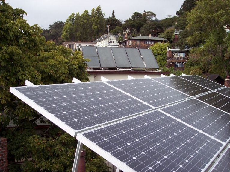
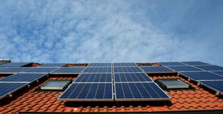
Solar Panels
Solar panels are the most common application of photovoltaic cells and are widely used to generate electricity for residential, commercial and industrial purposes. Solar panels can be installed on rooftops or integrated into building materials to provide on-site renewable power generation.
Satellites
Photovoltaic cells are used to power satellites and spacecraft, taking advantage of the abundant solar energy available in space. The high power to weight ratio of photovoltaic cells makes them ideal for providing power while minimizing launch weight.
Solar Cars
Some solar-powered cars and vehicles use photovoltaic cells, often in conjunction with battery storage, to partially or fully drive the vehicle. Photovoltaic cells provide emissions-free power from sunlight.
Off-Grid Power
In remote areas without access to an electricity grid, photovoltaic cells coupled with batteries can provide stand-alone power systems. These off-grid solar power systems are a clean and sustainable electricity source.