What Is The Working Principle Of Photovoltaic Effect?
The photovoltaic effect is the process by which a photovoltaic cell converts sunlight into electricity. When photons from sunlight strike the cell, they transfer their energy to the semiconductor material in the cell, causing electrons to break free and flow through the material to produce electric current. The photovoltaic effect was first observed by French physicist Edmund Becquerel in 1839.
Today, photovoltaic cells are used to produce solar power in a wide variety of applications. They can be found in small devices like calculators and watches, as well as in utility-scale solar farms and rooftop solar panel installations. The photovoltaic effect allows sunlight, a clean and readily available energy source, to be harnessed in an efficient and sustainable way to produce electricity on demand.
In this article, we will take a closer look at how the photovoltaic effect works, including the materials and components involved. We will examine the key mechanisms and processes that enable a photovoltaic cell to convert photonic energy into electrical energy. The efficiency and performance characteristics of PV cells will also be discussed.
History and Discovery of Photovoltaic Effect
The photovoltaic effect was first observed in 1839 by French physicist Alexandre-Edmond Becquerel. At just 19 years old, Becquerel conducted experiments with an electrolytic cell made up of two metal electrodes placed in an electrolyte solution. He found that small amounts of electricity were produced when the electrodes were exposed to light. This demonstration marked the first recorded observation of the photovoltaic effect.
Over the next several decades, more experiments were done to study this phenomenon. In 1873, Willoughby Smith discovered that selenium generates electricity when exposed to light. In 1876, William Grylls Adams and Richard Evans Day observed electricity generation when selenium was exposed to light. In 1877, William Adams and Richard Day built the first solar cell made from selenium wafers. In 1883, Charles Fritts created the first true solar cells by coating selenium with an extremely thin layer of gold to form the junctions.
In 1905, Albert Einstein published a paper that helped explain the photoelectric effect on a theoretical level. His work describing the nature and characteristics of light as particles, or photons, eventually won him the Nobel Prize in 1921 and laid important groundwork for harnessing solar power.
The development of modern solar cells began in 1954 when researchers at Bell Laboratories, Calvin Fuller, Daryl Chapin and Gerald Pearson, created the first silicon photovoltaic cell with a sunlight conversion efficiency of around 6%. Within a few years, their silicon solar cells were being used to power early space satellites launching in the late 1950s and 1960s.
Photovoltaic Materials
Photovoltaic cells are made from semiconductor materials that exhibit the photovoltaic effect. When light strikes these materials, photons are absorbed, energizing electrons and allowing them to flow freely, generating an electrical current. There are a few key properties that make a material suitable for photovoltaic applications:
- Bandgap Energy – The bandgap refers to the energy difference between the valence band (where electrons are bound to atoms) and the conduction band (where electrons can move freely). The ideal bandgap allows absorption of photons in the visible and UV spectrum of sunlight.
- High Absorption Coefficient – A high absorption coefficient means the material readily absorbs photons. This allows thinner material layers to be used.
- Minimal Recombination – Recombination refers to energized electrons falling back to lower energy states and releasing energy as heat. Minimal recombination increases efficiency.
- Carrier Mobility – Carrier mobility refers to how quickly energized electrons can move through the material. Higher mobility equals greater current.
Some of the most common photovoltaic materials used today include:
- Crystalline Silicon – This is the oldest and most widely used PV material. It has good light absorption and high carrier mobility.
- Gallium Arsenide – Has very high efficiency but is more complex and costly to manufacture.
- Cadmium Telluride – A thin-film technology with easier manufacturing but slightly lower efficiency.
- Copper Indium Gallium Selenide – Another thin-film option gaining popularity for flexibility and price advantages.
Mechanism
The photovoltaic effect is based on the interactions between photons of light and the electrons in a semiconductor material. When photons are absorbed by the material, they transfer their energy to the electrons. This extra energy excites the electrons and causes them to break free from their atomic bonds.
In a PV cell, a semiconductor material is specially treated to form an electric field that separates the excited electrons from the material atoms. One side of the cell becomes positively charged (the holes where electrons used to be) and the other side becomes negatively charged as the electrons accumulate there.
This separation of positive and negative charges across the cell creates a voltage difference, similar to a battery. An external circuit can then be connected to extract electric current and do work.
P-N Junction
A P-N junction forms the core of a photovoltaic cell. It consists of two semiconductor regions that are oppositely doped – one with an excess of positive charge carriers (p-type) and the other with an excess of negative charge carriers (n-type). This junction between p-type and n-type semiconductors sets up an electric field that enables the separation of photogenerated charge carriers.
In the p-type region, the majority charge carriers are holes, while electrons are the majority carriers in the n-type region. At the interface between the p and n-type regions, diffusion initially causes electrons to flow from the n-side to the p-side, and holes to flow from the p-side to the n-side. This diffusion of charge carriers leaves behind exposed charged atoms, creating a region at the junction called the depletion region which has a strong electric field.
When light shines on the solar cell and photons are absorbed in the p-n junction, electron-hole pairs are generated. The electric field at the depletion region separates these photo-generated electron-hole pairs before they can recombine. The electric field drives electrons to the n-side and holes to the p-side, producing a current that can be drawn from the solar cell.
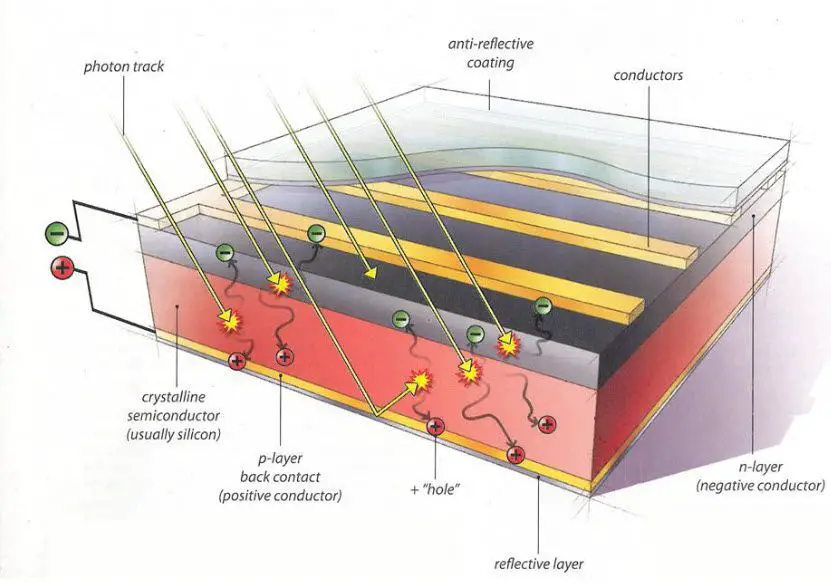
PV Cell Construction
A typical photovoltaic (PV) cell is made up of several critical components sandwiched between a top and bottom protective layer. Each layer serves an important function in converting sunlight into electricity through the photovoltaic effect.
The top layer is usually a transparent conductive oxide coating, like tin oxide, that allows sunlight to pass through while also conducting electricity. Under this is the N-type silicon layer which has an excess of electrons. Next is the P-N junction between the N-type and P-type silicon layers where the electric field is formed. The P-type silicon layer has electron holes or deficiencies. On the bottom is a back-side electric field layer which prevents carrier recombination and reflects sunlight back into the cell. Finally, a conductive metal backing like aluminum serves as the negative electrode.
When sunlight enters the cell, photons strike the N-type silicon and excite its electrons to jump the P-N junction barrier and enter the P-type layer. This flow of electrons creates the electric current while the buildup of holes in the N-type layer and excess electrons in the P-type layer generates the voltage. The transparent conductive oxide layer and metal backing act as connections to extract the current and voltage from the cell.
IV Curve
The current-voltage (IV) curve is one of the most important characteristics used to describe the behavior of a photovoltaic (PV) cell. It shows the relationship between the current through the cell and the voltage across the terminals under different conditions of illumination.
When no light shines on the cell, there is essentially no current. As the intensity of light increases, the current through the cell increases proportionally. The IV curve has a characteristic ‘knee’, indicating the maximum power point. At this point the product of current and voltage reaches its peak value.
Several key parameters can be obtained from the IV curve:
- Short circuit current (Isc) – current through cell when voltage is zero
- Open circuit voltage (Voc) – voltage across cell when current is zero
- Maximum power point (Vmp, Imp) – voltage and current at max power
- Fill factor (FF) – a measure of squareness of IV curve
- Efficiency – ratio of cell’s electrical power output to incident light power
These parameters help characterize the electrical performance of a PV device. The IV curve changes with irradiation and temperature, so it provides valuable insights into real-world operation.
Efficiency
The efficiency of a photovoltaic cell refers to what percentage of the solar energy striking the cell is converted into usable electricity. There are several factors that impact the efficiency of PV cells:
-
PV material – Different semiconductor materials have different conversion efficiencies, with more advanced multi-junction cells able to reach higher efficiencies than conventional silicon cells.
-
Temperature – Solar cell efficiency decreases as temperature increases. This is less of an issue with newer technologies like PERC solar cells.
-
Quality of semiconductor – Defects and impurities in the semiconductor can provide sites for electron-hole recombination which decreases efficiency.
-
Reflection off cell surface – Anti-reflective coatings help trap more light in the cell.
-
Resistance – High resistance leads to power loss and lower efficiency.
Typical efficiencies for commercial PV technologies are:
-
Mono-crystalline silicon – 15-20%
-
Poly-crystalline silicon – 13-16%
-
Thin-film (CdTe) – 8-12%
-
Thin-film (CIGS) – 10-12%
-
Multi-junction cells – 30-40%
Applications
Photovoltaic cells have become an indispensable source of renewable energy with applications spanning many sectors. Some major uses of PV cells today include:
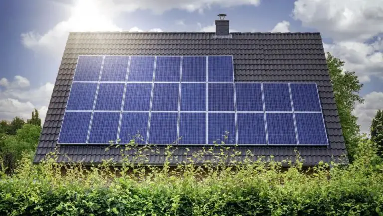
- Residential solar panels – Homeowners are increasingly installing rooftop solar systems to reduce their electricity bills and carbon footprint.
- Commercial and industrial solar farms – Large-scale solar panel farms provide clean electricity to the grid. Many companies are also installing solar arrays to power their operations.
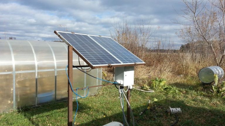
- Off-grid power systems – PV cells allow remote locations like satellites, road signs, cabins, boats and more to be energy self-sufficient.
- Solar vehicles – Cars, buses, trains and some aircraft are integrating solar panels to supplement their energy needs.
- Consumer electronics – Small solar cells provide power for watches, calculators, toys and portable chargers.
The solar PV market has experienced exponential growth in recent years. Total global installed capacity went from under 10 gigawatts in 2007 to over 500 gigawatts by 2018. This growth is expected to continue as solar electricity costs fall and climate change concerns mount. Emerging applications like building-integrated PV, solar powered drones, and solar desalination also hold promise for the future.
Future Outlook
The future looks bright for photovoltaics. Several emerging technologies and materials show promise for improving solar cell efficiency and lowering costs even further.
Perovskite solar cells have emerged as a promising thin-film PV technology, with lab efficiencies already exceeding 25%. Perovskites can be printed on flexible substrates, enabling new lightweight and portable applications. However, perovskites still face challenges with toxicity, stability, and scaling up manufacturing. With more research, perovskites could complement and enhance silicon solar cells.
Organic PV and dye-sensitized solar cells are other thin-film technologies aiming to achieve ultra-low production costs using roll-to-roll manufacturing. Lifespans and efficiencies continue improving. These technologies may find niche applications where flexibility, semi-transparency, or very low cost matter most.
Concentrated PV systems use mirrors and lenses to focus sunlight on small high-efficiency solar cells, reducing overall material needs. Tracking systems optimize orientation toward the sun. Further cost reductions are possible as concentration optics improve.
New materials like gallium arsenide, gallium phosphide, and indium gallium nitride are also being researched to replace silicon. These III-V semiconductors have greater light absorption and could achieve higher efficiencies, especially in multi-junction tandem cell configurations.
With so many innovations underway, analysts project solar PV installations will continue their rapid growth worldwide. Costs are expected to fall further, making solar ever more competitive with fossil fuels. The future is bright for photovoltaics contributing an increasing share of clean, renewable energy.