How Does A Photovoltaic Cell Work Step By Step?
A photovoltaic (PV) cell is an electrical device that converts light directly into electricity using the photovoltaic effect. PV cells are the building blocks of photovoltaic modules, otherwise known as solar panels. The purpose of a PV cell is to absorb photons from sunlight and convert that light energy into electricity through the photovoltaic effect. PV cells provide a clean, renewable way to generate electricity from sunlight.
Semiconductors
Semiconductors are materials that have electrical conductivity between that of insulators like glass and conductors like metals. This means that semiconductors can be switched between conducting or insulating electricity depending on conditions like temperature, illumination, and the introduction of impurities (dopants).
Some key properties of semiconductors are:
- Band gap – This is the energy range where no electron states can exist. The band gap separates the valence band (outer electrons) from the conduction band (free to move).
- Doping – Introducing impurities into the semiconductor can donate free electrons (n-type) or electron holes (p-type). This increases conductivity.
- Photoconductivity – Illumination with photons of energy greater than the band gap can excite electrons into the conduction band, creating more free electrons and holes to conduct electricity.
Common semiconductor materials used in electronics include silicon, germanium, and gallium arsenide. Understanding the properties of semiconductors is key to explaining how photovoltaic cells work.
PN Junction
A PN junction is formed when a p-type semiconductor and an n-type semiconductor are brought into contact with each other. When this happens, diffusion of electrons occurs from the region of high electron concentration (the n-type side) into the region of low electron concentration (the p-type side). Similarly, diffusion of holes occurs from the p-type side to the n-type side. When an electron diffuses into the p-type material, it combines with a hole. Similarly when a hole diffuses into the n-type side, it combines with an electron. This diffusion of charge carriers causes a depletion region around the junction as these mobile charge carriers move away.
The depletion region consists of immobile, fixed ions with a certain electric field profile. The electric field arises due to the imbalance of charge on either sides of the junction. There is a built-in potential across this depletion region proportional to the difference between the Fermi levels of the p-type and n-type materials. This built-in potential acts as a barrier, preventing further diffusion of excess carriers across the junction. Only when sufficient external voltage is applied in the reverse biased condition can this potential barrier be overcome.
Absorbing Light
When light hits the solar cell, photons with enough energy are absorbed by the semiconductor material. This photon absorption leads to electrons breaking free from their bonds and leaving behind positively charged holes. Specifically, when a photon hits an electron in the valence band of the semiconductor, the energy can excite the electron up into the conduction band. This promotion of electrons from the valence band to the conduction band is what generates electron-hole pairs.
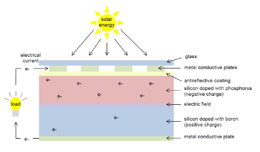
The key property of semiconductors that enables this light absorption process is their bandgap. The bandgap is the energy difference between the valence band and conduction band in a semiconductor. When a photon with energy greater than or equal to the bandgap hits the solar cell, it will be absorbed and create an electron-hole pair. Photons with less energy than the bandgap will pass through the material without being absorbed.
The number of electron-hole pairs generated is directly proportional to the intensity and wavelength of the incoming sunlight. More intense sunlight, especially at wavelengths tuned to the bandgap, will generate more electron-hole pairs. This is the initial step in the photovoltaic effect that ultimately leads to electricity generation.
Electric Field
When light hits the solar cell, it knocks electrons loose in the semiconductor material, creating electron-hole pairs. The PN junction separates these positive and negatively charged carriers, forming an electric field across the junction. This builds up voltage potential, similar to a battery.
The built-in electric field provides the voltage needed to drive current through an external load, creating useable electricity. The electrons are pushed by the electric field to travel to the N-side and holes to the P-side. This movement of charge carriers across the junction due to the electric field is called “drift current.”
The strength of the electric field depends on the properties of the PN junction materials. Careful selection of the semiconductor can maximize the magnitude of the built-in electric field, improving solar cell efficiency.
External Circuit
The external circuit of a photovoltaic cell provides a path for electrons to travel through and do work. When light hits the semiconductor and causes electrons to flow, those electrons move from the N-type layer to the P-type layer within the cell. However, they cannot reach the back contact due to the electric field created by the PN junction. The only place for the electrons to go is through the external circuit.
The front contact is connected to a wire or electrical component that allows a path for the electrons to flow through. As the electrons exit the front contact, they travel through the external wire or component and back to the rear contact. This flow of electrons through the external circuit is an electric current that can then be harvested and utilized. For example, the current may power an appliance, be stored in a battery, or fed into the electric grid.
Without an external circuit, the electrons would have nowhere to go and no work could be extracted from the PV cell. The external circuit provides the crucial path for electron flow and current to be generated from the PV cell.
Characterizing Solar Cells
Solar cell performance is characterized using several key parameters:
Open-Circuit Voltage (VOC) – This is the maximum voltage available from a solar cell, measured when no current is flowing. VOC represents the amount of forward bias on the solar cell due to the bias of the solar cell junction with the light-generated current.
Short-Circuit Current (ISC) – This is the current through the solar cell when the voltage across it is zero (when it is short circuited). ISC directly depends on the amount of sunlight hitting the solar cell.
Fill Factor (FF) – This is defined as the ratio of the maximum power from the solar cell to the product of VOC and ISC. The fill factor is a measure of the “squareness” of the IV curve and is always less than 1.
Efficiency – This is the ratio of electrical power output from the solar cell to input power from the sunlight. Efficiency depends on VOC, ISC, and FF and indicates how much of the solar energy is converted into electrical energy.
By measuring and optimizing these parameters, solar cell performance can be characterized and maximized.
Connecting Solar Cells
To generate useful amounts of electricity, solar cells are connected together to form larger solar panels and arrays. Individual solar cells typically only generate about 1-2 watts of power, which isn’t enough for most applications. By wiring cells together in series and parallel circuits, higher voltages and currents can be achieved.
In a series connection, solar cells are daisy chained together and the voltage adds up across each cell. For example, connecting two 0.5V cells in series produces 1V. However, the current stays the same. In a parallel connection, the cells are connected side-by-side and the current adds up across each cell, while the voltage stays the same. For example, two cells in parallel rated at 0.5V and 1A would produce 0.5V and 2A.
Modules consist of solar cells wired together and protected by a glass covering and aluminum framing. Modules are typically rated from 10 to 400 watts. Panels are made up of multiple modules assembled together into a single pre-wired structure. Arrays are comprised of multiple panels connected together to generate electricity at utility-scale levels.
When connecting modules and panels into arrays, blocking and bypass diodes are used to prevent damage from shading and system mismatches. Optimizers and micro-inverters can also be used at the panel level to maximize energy harvest from each panel.
Applications
Solar photovoltaic (PV) cells have a wide variety of applications that take advantage of their ability to convert sunlight directly into electricity. Here are some of the most common applications of solar PV technology:
Residential solar: Homeowners are increasingly installing solar panels on their rooftops to generate electricity and reduce their dependence on the grid. Typical residential systems are in the range of 3-8 kilowatts and can provide a portion of a home’s electricity needs.
Commercial solar: Businesses, warehouses, retail stores, and other commercial buildings also commonly install PV systems to offset their electricity usage. Commercial-scale solar farms can range from tens to hundreds of kilowatts.
Utility-scale solar: Large solar farms owned by utilities generate massive amounts of solar electricity to feed into the grid. Some can exceed 100-150 megawatts in capacity.
Off-grid solar: Solar PV can provide electricity in remote locations without access to the grid, such as remote homes, communications towers, and more. Off-grid systems require batteries to store excess solar energy for nighttime use.
Solar vehicles: Solar panels are used to partially or fully recharge the batteries in electric vehicles and boats. Covering a vehicle’s surface with PV cells can extend driving range.
Spacecraft: Solar provides abundant electricity for satellites, space stations, and other spacecraft. Solar energy doesn’t get depleted like chemical fuels.
Consumer electronics: Small solar cells provide power for calculators, watches, battery chargers, and an array of compact electronics.
Future Outlook
The future looks bright for improvements in photovoltaic cell technology and increased adoption of solar power. Here are some key areas where we can expect to see innovations:
Efficiency: Researchers are working to push the limits of solar cell efficiency, targeting above 30% conversion rates. Approaches include multi-junction cells, intermediate bandgaps, hot carrier cells, and improved semiconductor materials.
Manufacturing: New high-throughput manufacturing techniques like roll-to-roll processing can reduce production costs through automation, speed, and material utilization. Economies of scale will further drive down costs.
New Materials: Emerging thin-film materials like perovskites and quantum dots show promise to replace silicon as the light absorber. These materials can enable flexible, lightweight solar panels.
Novel Designs: Concepts like solar paints, solar windows, and solar roofs could help seamlessly integrate photovoltaics into buildings and infrastructure. Advances in nanotechnology may enable such creative applications.
Storage Integration: Pairing solar panels directly with storage like batteries can provide 24/7 clean electricity on demand. Solar+storage systems will help expand the technology’s capabilities.
With these innovations, solar power is poised to become an increasingly significant portion of the global energy mix and play a key role in the transition to sustainable energy.