How Do Photovoltaic Cells Produce Energy?
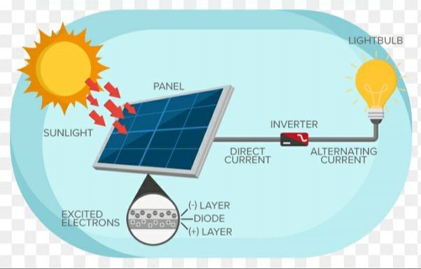
Photovoltaic cells, often referred to as solar cells, are devices that convert light energy directly into electrical energy. They are commonly used in solar panels to produce electricity from sunlight. The word “photovoltaic” comes from “photo,” meaning light, and “voltaic,” meaning electricity. So photovoltaic cells produce voltage and electric current when exposed to light.
Solar energy from photovoltaic systems is an important renewable energy source. With concerns about climate change and finite fossil fuel supplies, photovoltaics provide a clean alternative for generating electricity. Solar cells are now used in a wide variety of applications, from small consumer electronics to large utility-scale solar farms.
The basic physical process behind how a photovoltaic cell works is the photovoltaic effect. Photons from sunlight strike the solar cell and are absorbed by semiconductor materials in the cell, knocking electrons loose. This generates an electric current that can be captured and used as electricity. We’ll explore the photovoltaic effect and the components of a solar cell in more detail throughout this article.
Structure
Photovoltaic cells are made up of several key components that enable them to absorb sunlight and convert it into electricity. At the most basic level, PV cells contain two layers of semiconductor material, typically silicon, that have been altered to form a positive and negative layer (known as a PN junction). The top layer is treated to be positively charged, while the bottom layer is treated to be negatively charged.
When sunlight hits the solar cell, photons from the light excite the electrons in the negative layer and cause them to flow through an external circuit to the positive layer, generating an electric current. The PN junction is critical to forming the electrical field that forces electrons to flow in one direction.
In addition to the semiconductor layers, solar cells have a top electrode layer that collects the electrons as they flow through the external circuit. An antireflective coating is also added to the top layer of cells to reduce reflective loss of sunlight hitting the surface. Metal conductive plates on the bottom and top act as connections to the circuit.
Semiconductor Materials
Photovoltaic cells require semiconductor materials that exhibit the photovoltaic effect. The most common material used is silicon. Silicon atoms bond together to form a crystal structure with unique electrical properties. With just the right amount of impurities added, silicon can be tuned to be an excellent semiconductor.
Silicon cells dominate the PV market, making up over 90% of cells produced globally. However, thin-film materials like cadmium telluride (CdTe) are gaining traction as a lower-cost alternative. CdTe absorbs sunlight efficiently, allowing thin flexible cells to be produced. The toxicity of cadmium does raise environmental concerns though. Other thin-film materials like Copper Indium Gallium Selenide (CIGS) are also being explored.
The choice of semiconductor material impacts solar cell efficiency and cost. Silicon remains popular for striking a good balance, but alternatives continue to emerge. The material science behind photovoltaics is key for optimizing performance.
PN Junction
A PN junction is the interface between a P-type semiconductor and an N-type semiconductor. Semiconductors are materials that have electrical properties between conductors and insulators. Silicon and germanium are commonly used semiconductor materials in photovoltaic cells.
These materials are “doped” with other elements to create the P and N regions. P-type semiconductors are doped with elements that have fewer valence electrons, creating “holes” with a positive charge. N-type semiconductors are doped with elements that have more valence electrons, creating excess negative charges from the electrons.
When the P-type and N-type semiconductors are joined together, electrons diffuse from the N side to the P side, while holes diffuse from the P side to the N side. This diffusion creates a region at the junction called the depletion zone that has no free charge carriers. The imbalance of charges between the P and N regions creates an electric field across the depletion zone.
This electric field provides the driving force to separate photogenerated electrons and holes when light shines on the material, enabling current to flow when the PV cell is connected to an external load.
Photon Absorption
Photovoltaic cells rely on the photoelectric effect to produce electricity. When photons from sunlight hit the solar cell, they transfer their energy to the semiconductor material. If the photon has enough energy, it can excite an electron in the material’s atom to jump from the valence band to the conduction band. This leaves behind a positively charged hole in the valence band. The energy provided by the photon must be equal to or greater than the band gap of the semiconductor in order to excite the electron to the conduction band. The band gap is the minimum energy required to dislodge an electron from its bound state.
Silicon is commonly used in solar cells and has a band gap energy of 1.1 electronvolts (eV). Photons with energy below this value will pass through the cell. Photons with energy above 1.1 eV will be absorbed, and the excess energy above the band gap will heat up the cell. Therefore, photons with energy as close to the band gap as possible are ideal for generating electricity efficiently. When the excited electron jumps to the conduction band, it leaves behind a “hole” with positive charge. This creates an electric field across the cell, causing electrons to flow in one direction, resulting in an electrical current that can be harvested.
Electron Flow
When photons are absorbed in the solar cell, they transfer their energy to electrons in the semiconductor material’s atoms. This energizes the electrons, freeing them from their atomic bonds and allowing them to flow through the material as electricity.
Specifically, in the PN junction of the solar cell, the absorption of light generates electron-hole pairs. The built-in electric field across the PN junction causes these electrons and holes to drift in opposite directions – electrons to the N-type side and holes to the P-type side. This separation of charge creates a voltage difference, or photovoltage.
When the two sides of the PN junction are connected in an external circuit, it allows the electrons to flow through that external circuit, generating electrical current. This current generation continues as long as light is absorbed by the solar cell and electron-hole pairs are created.
Efficiency
The conversion efficiency of a photovoltaic cell is a measure of how much of the sun’s energy striking the cell is converted into usable electricity. It is expressed as a percentage of the total solar irradiance that is converted.
There are several factors that limit the efficiency of photovoltaic cells:
- Reflection losses – Some of the incoming sunlight is reflected off the surface of the cell and lost.
- Recombination losses – When light generates electron-hole pairs, some recombine before being extracted as current.
- Resistive losses – The semiconductor material has some electrical resistance that dissipates power.
- Photon energy loss – Photons with energy higher than the band gap are wasted, generating heat.
- Shading losses – Parts of the cell that are shaded produce less current.
Typical commercial silicon solar cells have efficiencies around 15-20%. Higher efficiency can be achieved by using multi-junction cells, concentrating sunlight, or other advanced techniques, but this comes at higher cost.
Manufacturing
The manufacturing process for photovoltaic cells involves several key steps. First, the raw semiconductor materials, typically silicon, must be refined and formed into ingots or bricks. This involves heating and melting polysilicon feedstock, then allowing it to cool and solidify into a large crystalline ingot.
The ingots are then cut into thin wafers using wire saws or other specialized cutting equipment. Wafers are usually between 150-200 microns thick. The wafers are then polished, cleaned, and undergo surface texturing to optimize light absorption.
The wafers then go through diffusion furnaces to embed the p-n junction. Additional layers may be added to the cell, such as anti-reflective coatings and electrical contacts. Cells are interconnected and assembled into modules and panels.
Throughout the manufacturing process, rigorous testing takes place to ensure quality and performance. Cells are tested under simulated sunlight and for durability under various environmental conditions. Performance optimization, waste minimization, and cost reduction are continual goals of PV cell fabrication.
Applications
Photovoltaic cells have many practical applications and are used in a variety of settings:
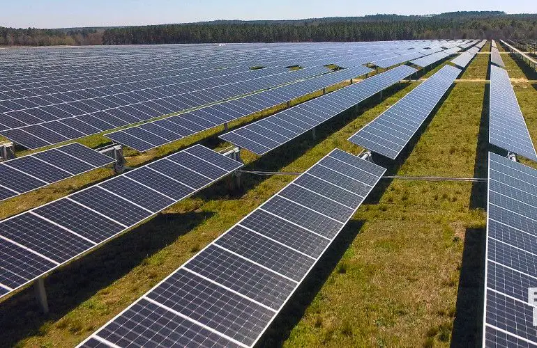
– Solar farms – Large-scale solar power plants that contain thousands of photovoltaic panels spread over acres of land. The electricity generated is fed into the power grid to supply energy to homes, businesses and industries.
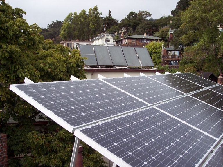
– Rooftop solar – Photovoltaic panels installed on the rooftops of residential and commercial buildings to generate electricity. This allows households and businesses to produce some or all of their own electricity needs.
– Satellites and spacecraft – Photovoltaic cells are the main source of power for satellites and provide electricity for communications, observation, and weather monitoring from space.
– Consumer electronics – Small photovoltaic cells can power watches, calculators, toys and battery chargers by converting light energy into electricity.
– Off-grid applications – Photovoltaic systems allow electricity generation in remote locations where connection to the power grid is not possible, such as isolated homes, boats, lighthouses, and more.
– Solar vehicles – Cars, planes, boats can be powered by photovoltaic cells, especially in solar-powered races and competitions.
Future Outlook
The future looks bright for photovoltaic technology. There are several key areas where we can expect to see improvements in the coming years:
Improving Efficiency
Researchers are working to improve the efficiency of photovoltaic cells, which currently max out around 22% for commercial silicon cells. Some experimental designs have reached over 40% efficiency in lab settings. With improved materials and nanostructuring techniques, we may see 30%+ efficient solar panels commercially available within 5-10 years.
Emerging Designs
Beyond traditional silicon cells, other designs like thin-film, organic PV, and multi-junction cells offer unique benefits. Thin-film cells use very little material and can be flexible, while multi-junction cells can capture more of the solar spectrum by using multiple stacked semiconductor layers. Organic PV offers a low-cost option using carbon-based materials. These emerging designs will open up new applications for solar power.
Growth Trends
Solar power has grown enormously over the past decade, nearly doubling global installed capacity every couple years. This exponential growth is expected to continue as costs fall and solar matches or beats fossil fuels on cost in more locations. Supportive government policies and technological advances will drive adoption of solar power worldwide.